Views: 0 Author: Site Editor Publish Time: 2025-12-09 Origin: Site


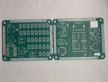
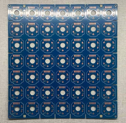
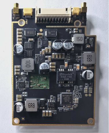
As a professional PCB manufacturer, we’ve been focusing on high-precision PCB customization—and today, we’re proud to showcase our flagship product for Single-Photon Avalanche Diode (SPAD) imaging detectors: the optical chip substrate (a high-end type of IC Carrier PCB).
SPADs are game-changers in fields like astronomy, quantum computing, and biological imaging, and their performance relies heavily on the supporting PCB. The biggest manufacturing challenge of this board lies in its two "two-step staircases": we use depth-controlled routing twice plus laser opening to shape them, with strict depth tolerance—any tiny error would lead to scrapping.
To ensure reliability, we adopt NiPdAu Plating for the surface—this PCB-specific process delivers strong adhesion and anti-peeling performance, perfect for harsh working environments. As a high-end High-Precision PCB, its circuit design is ultra-fine: 2mil line width and spacing, plus 0.070mm minimum bonding pad, maximizing integration while ensuring stable signal transmission.
Unlike ordinary PCBs, IC Carrier PCB like this one depends on extreme precision in every detail—from substrate selection to process control. It’s this focus on PCB craftsmanship that makes our products trusted by clients in high-tech industries.
Need custom High-Precision PCB or IC Carrier PCB? feel free to reach out—we’re here to help!
—we’ll turn your requirements into high-quality PCBs!