Views: 0 Author: Site Editor Publish Time: 2025-11-26 Origin: Site


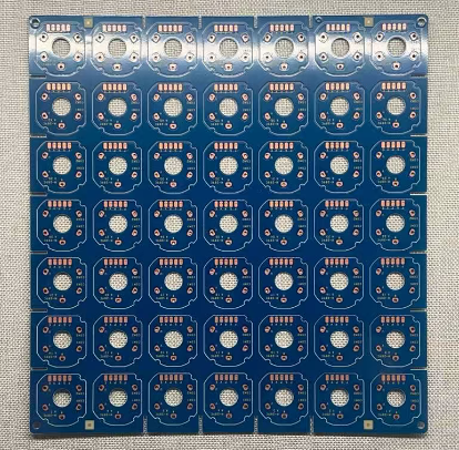
Recently, we successfully completed a custom optical module PCB for Amphenol, which meets the strict performance requirements of optical modules in communication equipment with high-spec craftsmanship and precise parameters. The physical finished products have passed Amphenol’s quality verification.
Core PCB Customization Specifications: Tailored for Optical Module Demands
This PCB custom-made for Amphenol is designed to support the complex signal links and structural compatibility of optical modules, with key configurations as follows:
Structure & Layer Count: 8-layer 3-step design, accommodating the interlayer layout needs of the optical module’s complex signal paths;
Material & Process: Adopting EM-892K2 material to ensure stable transmission of high-frequency signals in optical modules; the surface uses ENIG 2U” + gold finger 30U” process—ENIG 2U guarantees oxidation resistance and signal contact stability, while 30U gold fingers significantly enhance the durability of interface plugging/unplugging;
Board Thickness & Appearance: Board thickness is precisely controlled at 1.05±0.1mm (targeted at 1.0mm), matching the compact space constraints of optical modules; the appearance features a blue substrate + white silkscreen to clearly display on-board interface information, complying with Amphenol’s labeling standards.
Optical Module PCB Application: Craftsmanship Assurance for High Requirements
Optical modules are core transmission components in data centers and communication base stations, requiring high PCB signal integrity and interlayer precision. This 8-layer 3-step PCB effectively reduces signal interference and ensures the high-speed data transmission performance of optical modules through precise stack-up design and process control. The neat interfaces and uniform plating of the physical board also reflect our attention to detail for high-end clients’needs.
As a manufacturer focusing on high-end PCB customization, we cover custom needs in fields like optical modules, industrial control, and communication equipment, providing end-to-end services from material selection to process implementation.