Views: 0 Author: Site Editor Publish Time: 2026-02-26 Origin: Site


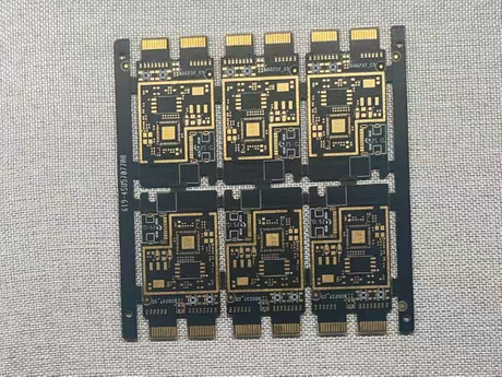
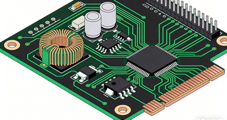
For consumer electronics and next-gen devices demanding ultra-fast data transfer, our 10-layer 4-step HDI PCB delivers unmatched performance. Built with FR-4 substrate, 1.4mm thickness, and 0.1mm fine routing, it features 50µm laser-drilled microvias and ENIG surface finish, enabling 40Gbps+ signal transmission. Its 4-step sequential lamination cuts signal paths by 58%, supporting 01005 components and 0.35mm pitch BGA for extreme density.
Ideal for 5G RF front-end modules, 8K video encoders, AI edge processors, and ADAS sensor arrays, this PCB ensures precision impedance control and 0.8µm surface flatness. Whether you’re building XR headsets or 400G network switches, it’s engineered for high-speed, high-reliability performance.
Ready to elevate your high-bandwidth device? Contact our team today to request a custom PCB.