Views: 0 Author: Site Editor Publish Time: 2026-03-02 Origin: Site


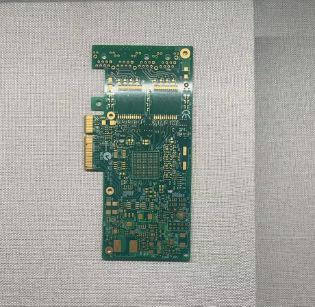
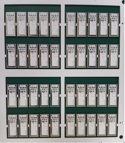
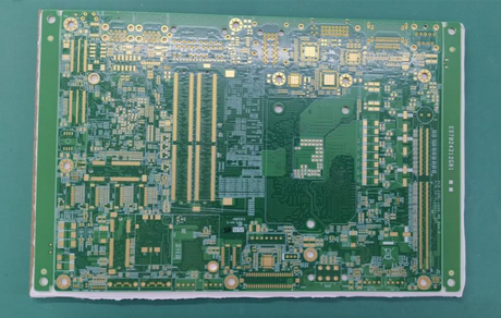
For next-generation 5G networks requiring ultra-reliable, high-bandwidth performance, our 10-layer 5G communication PCB delivers. Built with S1000-2 substrate, 2.0mm thickness, and 0.075mm precision routing, it features immersion gold + electroless gold 30, finish for superior signal integrity and corrosion resistance.
Engineered with low dielectric loss materials and a multi-layer design, it supports high-density interconnects (HDI) and efficient thermal management, ensuring stable performance for 5G base stations, wireless systems, network routers, and IoT gateways. Whether you’re building macro cells or small-cell deployments, this PCB is optimized for the rigorous demands of 5G infrastructure.
Ready to accelerate your 5G network deployment? Contact us today to request a custom quote or full technical datasheet.