Views: 0 Author: Site Editor Publish Time: 2026-01-07 Origin: Site


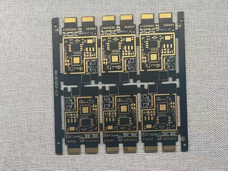
When hardware projects move beyond simple designs into the world of AI processors, 5G modules, and XR headsets, a basic board won't suffice. You need a high-speed engine that manages signal integrity as much as it saves space. This is where our 10-layer FR-4 PCB steps in—a powerhouse built for the industry’s most demanding tech.
Engineering Precision
What makes this board elite is the Advanced Manufacturing logic. We utilize 4-Step Microvias, involving three laser drills and two press cycles to allow for any-layer connectivity. This drastically shortens signal paths, which is essential for 400G network switches.
Key features include:
· Via Tech: 50-80μm laser holes with a 1:0.8 aspect ratio for ultra-fine routing.
· Zero Lag: Delay Matching keeps signal skew under 5ps in differential pairs.
· 3D Validation: Every layout is optimized using Ansys HFSS simulation.
Built for Reliability
With a 1.4mm thickness and a sleek black oil finish, this board is as rugged as it is smart. The Immersion Gold treatment ensures perfect solderability for dense components in ADAS sensor arrays or 8K encoders.
Ready to innovate? Contact us today to bring your high-density project to life.