In the intricate world of modern electronics, printed circuit boards (PCBs) stand as a fundamental and indispensable component. They serve as the foundation upon which countless electronic devices are built, enabling the seamless operation of everything from the tiniest wearable gadgets to the most powerful supercomputers.
Definition and Basic Concept
A printed circuit board is a flat, rigid board made of insulating material, typically fiberglass or a similar composite. It is printed with conductive pathways, usually made of copper, that are precisely etched onto its surface or embedded within its layers. These conductive traces act as the "wires" of the circuit, connecting various electronic components such as resistors, capacitors, transistors, integrated circuits, and more. The purpose of a PCB is to provide a physical platform for mounting these components and to establish the necessary electrical connections between them, allowing for the flow of electrical signals and the implementation of complex circuits.
Structure and Components
The structure of a PCB can vary depending on its complexity and application. At a basic level, it consists of a substrate, which provides mechanical support and electrical insulation. On top of the substrate, the conductive layers are formed. In a single - sided PCB, there is only one layer of conductive traces, usually on one side of the board. This type of PCB is relatively simple and cost - effective, commonly used in basic electronic devices like simple calculators or small - scale hobby projects.
Double - sided PCBs, as the name implies, have conductive traces on both sides of the board. To connect the traces on the two sides, small holes called vias are drilled through the board and plated with metal. These vias act as bridges, allowing electrical signals to pass from one side of the board to the other. Double - sided PCBs are more versatile and can accommodate more complex circuits compared to single - sided ones. They are widely used in consumer electronics such as smartphones, tablets, and many household appliances.
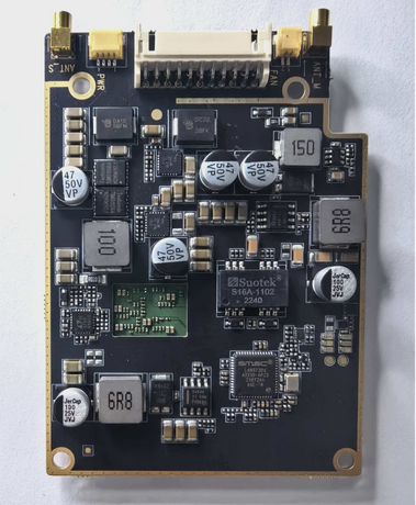
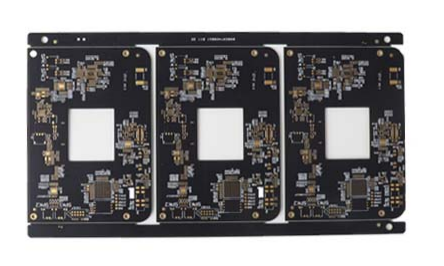
For even more complex applications, multilayer PCBs are employed. These boards contain multiple layers of conductive traces, separated by insulating layers. The additional layers provide more space for routing signals and power, enabling higher component density and more intricate circuit designs. Multilayer PCBs are essential in high - performance computing, telecommunications equipment, and aerospace electronics, where the need for compact, reliable, and high - speed circuitry is crucial.
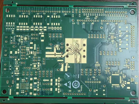
In addition to the substrate and conductive layers, PCBs also often include other components. The solder mask is a thin, protective layer applied over the conductive traces. It is usually green (although it can come in other colors), and its main function is to prevent solder from adhering to unwanted areas during the soldering process, thus reducing the risk of short circuits. The silkscreen layer, on the other hand, is used to print labels, component designations, and other useful information on the board. This helps in the assembly, testing, and maintenance of the PCB by making it easier to identify components and their functions.
Functions and Significance
The functions of PCBs in modern electronics are multi - fold and of utmost importance. Firstly, they simplify the assembly process of electronic devices. Instead of manually wiring each component together, which would be extremely time - consuming, error - prone, and difficult to scale up for mass production, PCBs allow for the standardized and automated placement and soldering of components. This not only increases the speed of production but also improves the reliability and consistency of the final product.
Secondly, PCBs play a crucial role in signal transmission. The carefully designed conductive traces on the board are engineered to minimize signal interference and distortion, ensuring that electrical signals can travel accurately and efficiently between components. In high - speed applications, such as in modern data communication systems where signals need to travel at very high frequencies, the design of the PCB's traces, including their length, width, and spacing, becomes even more critical. Special techniques, such as impedance matching, are employed to optimize signal integrity and prevent signal reflections that could degrade the performance of the system.
Moreover, PCBs contribute to the miniaturization of electronic devices. By providing a compact and organized platform for component integration, they enable the packing of more functionality into smaller spaces. This has been a driving force behind the development of today's portable and wearable electronics, where size and weight are key considerations. For example, in a modern smartphone, a highly complex PCB houses all the essential components, including the processor, memory, wireless communication modules, and sensors, in a space - efficient manner, allowing the device to be sleek and lightweight while still offering a wide range of advanced features.
In conclusion, printed circuit boards are the unsung heroes of the electronics industry. Their simple yet ingenious design has revolutionized the way electronic devices are manufactured, assembled, and operate. As technology continues to advance at a rapid pace, the demand for more sophisticated, compact, and high - performance PCBs will only increase. Engineers and researchers are constantly exploring new materials, manufacturing techniques, and design strategies to push the boundaries of what PCBs can achieve, ensuring that they will remain at the heart of modern electronics for years to come.