Views: 0 Author: Site Editor Publish Time: 2025-12-10 Origin: Site


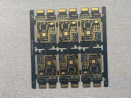
Let's dive into a key term for ceramic PCBs that every manufacturer and buyer should know: the etch factor. First, let’ ground this in the type of ceramic PCB we’re focusing on—Direct Bonded Copper (DBC) boards. These are composite workhorses: highly insulating alumina or aluminum nitride ceramic bonds directly with copper, formed by heating to 1065–1085°C. At this temp, copper oxidizes and diffuses with the ceramic to create a strong eutectic bond.
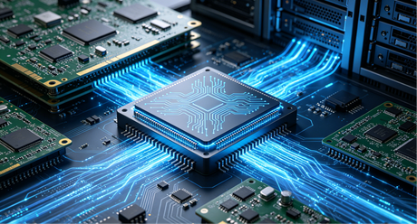
The DBC manufacturing flow keeps precision front and center: from raw material cleaning and oxidation to sintering, photolithography (film, exposure, development), etching, and final inspection. Etching is where the magic (and precision) happens—it’s the process that carves circuits by stripping unprotected copper.
Here’s the breakdown on etch factor: Chemical etchants don’t just etch straight down—they also eat away at the copper’s sides (lateral etching). The etch factor (F) quantifies this: we define it as the ratio of etching depth (T) to lateral etch width (A), so F=T/A. This balance matters because sharp, controlled circuits rely on a strong etch factor. Most DBC manufacturers require F>2 to ensure quality.
Curious how etch factor shifts impact ceramic PCB performance? Stay tuned for Part 2.