loading


| Availability: | |
|---|---|
| Quantity: | |
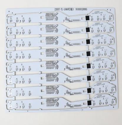
A four layer inner and outer layer 2OZ copper thick PCB circuit board is a high-performance and highly reliable multi-layer circuit board widely used in communication equipment, power modules, automotive electronics, industrial control and other fields. This PCB circuit board provides higher current carrying capacity and heat dissipation performance through a four layer design and 2OZ copper thickness, meeting the needs of high-power and high-density circuits. The following is a detailed introduction to the four layer inner and outer layer 2OZ copper thick PCB circuit board product.
Product Overview
A four layer inner and outer layer 2OZ copper thick PCB circuit board is a high-performance and highly reliable multi-layer circuit board widely used in communication equipment, power modules, automotive electronics, industrial control and other fields. This PCB circuit board provides higher current carrying capacity and heat dissipation performance through a four layer design and 2OZ copper thickness, meeting the needs of high-power and high-density circuits. The following is a detailed introduction to the four layer inner and outer layer 2OZ copper thick PCB circuit board product.
Product Features
2.1 High reliability
Using high-quality substrates and advanced manufacturing processes to ensure the reliability of PCBs in harsh environments such as high temperature, high humidity, and high vibration.
2.2 Excellent heat dissipation performance
By designing with a thickness of 2OZ copper, the heat dissipation capability of the PCB is significantly improved to meet the needs of high-power circuits.
2.3 High conductivity
The thickness of 2OZ copper can provide better conductivity, reduce the resistance of the circuit board, and improve the overall performance of the system.
2.4 High anti-interference ability
By rational circuit design and shielding technology, the anti electromagnetic interference capability of PCB is improved to ensure the stability and accuracy of signal transmission.
2.5 High integration
A four layer design can achieve higher circuit integration, reduce system complexity and volume, and improve overall performance and reliability of the system.
Technical Specifications
Number of layers: 4
Plate thickness: 1.6mm
Board: S1141
Copper thickness: inner and outer layers of 2OZ
Minimum line width and spacing: 0.3/0.3MM
Minimum aperture: 0.3
Surface treatment: lead-free tin spraying
Application field
4.1 Communication equipment
Used for circuit control and signal transmission of communication equipment, providing high reliability and high-performance circuit solutions.
4.2 Power module
Used for circuit control and power transmission of power modules, ensuring efficient energy conversion and stable output.
4.3 Automotive Electronics
Used for circuit control and signal transmission in automotive electronic systems, providing highly reliable and long-lasting electronic solutions.
4.4 Industrial Control
Used for circuit control and signal transmission in industrial control systems to ensure system stability and reliability.
4.5 Other high-power circuits
Used for circuit control and signal transmission in other high-power circuits, such as LED drivers, power tools, etc.
manufacturing process
5.1 Circuit Design
Use EDA tools for circuit design and wiring to ensure the rationality and reliability of the circuit.
5.2 Material selection
Choose high-quality substrates and copper foils to ensure the performance and reliability of the PCB.
5.3 Etching
Etching is performed to form a circuit pattern.
5.4 Vias
Drill holes and perform electroplating to form vias.
5.5 Layering
Layer four layers of copper foil and substrate together to form a four layer PCB.
5.6 Surface Treatment
Perform surface treatments such as HASL, ENIG, etc. to improve the soldering performance and corrosion resistance of PCBs.
5.7 Welding
Weld the components and complete the assembly.
5.8 Testing
Conduct electrical and functional testing to ensure product quality.
quality control
6.1 Raw material inspection
Ensure that the quality of the substrate and copper foil meets the standards.
6.2 Manufacturing Process Control
Strictly control every process to ensure product consistency and reliability.
6.3 Finished product testing
Conduct electrical performance testing, functional testing, and environmental testing to ensure that the product meets design requirements.
Conclusion
Four layer inner and outer layer 2OZ copper thick PCB circuit boards are widely used in various high-power and high-density circuits due to their high reliability, excellent heat dissipation performance, and high conductivity. Through rational design and strict manufacturing processes, efficient and reliable circuit solutions can be achieved to meet diverse electronic system requirements.


