loading
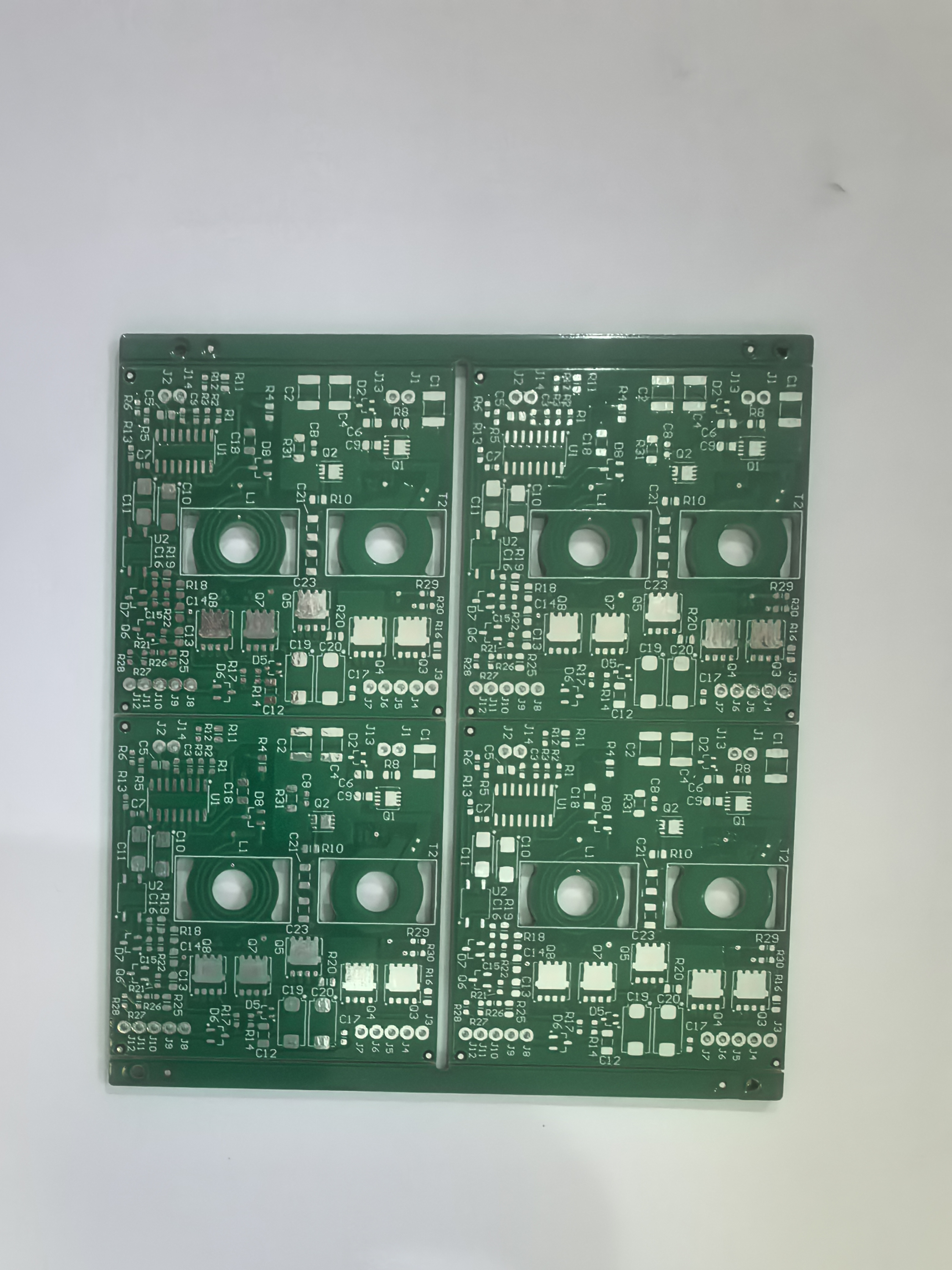
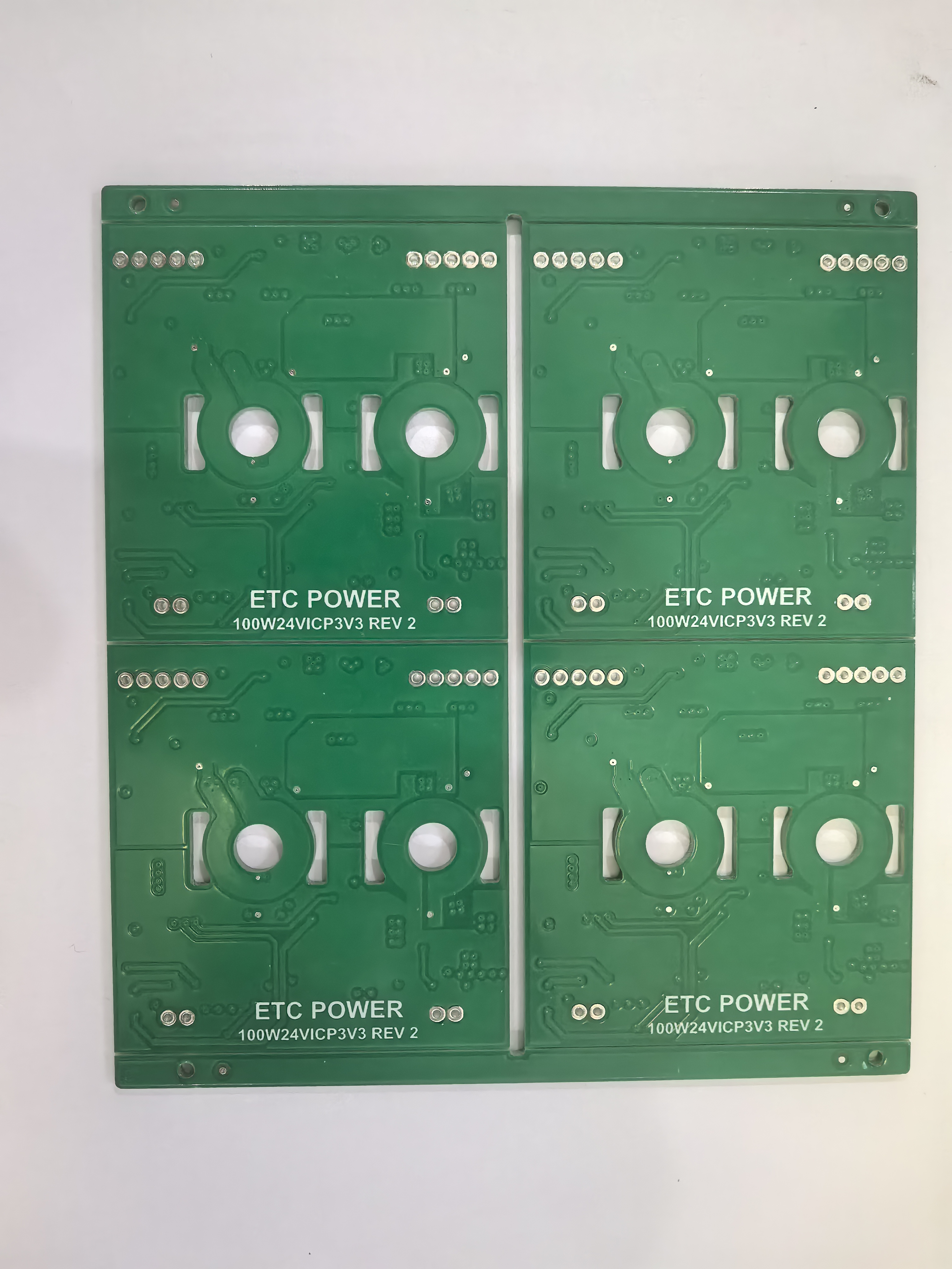
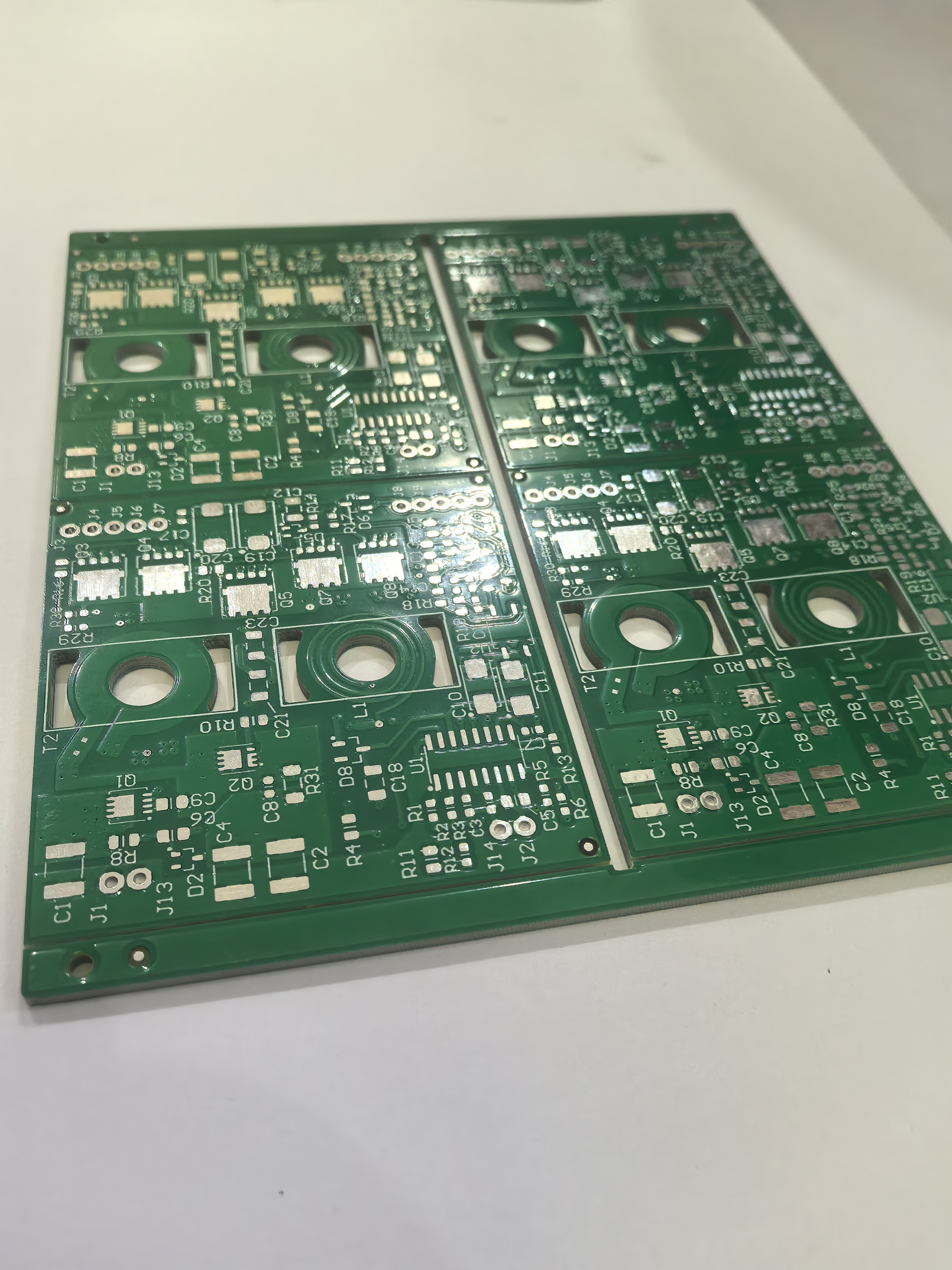
An 8-layer thick copper power PCB (printed circuit board) is a circuit board designed specifically for high-power and high-frequency applications, with excellent electrical performance and heat dissipation capabilities. Its multi-layered structure and thick copper layer make it an ideal choice for fields such as power management, industrial equipment, and communication systems.
Product Features
Multi layer structure: Adopting an 8-layer design, it can achieve complex circuit layouts, provide higher signal integrity and electrical performance.
Thick copper layer: Copper thickness is usually 2 oz (about 70 μ m) or higher, capable of carrying larger currents and suitable for high-power applications.
Superior heat dissipation performance: The thick copper layer design helps to dissipate heat quickly, reduce circuit board temperature, and improve system stability and reliability.
High frequency performance: Suitable for high-frequency signal transmission, reducing signal attenuation and crosstalk, ensuring signal stability.
Durability: Made of high-quality materials with excellent corrosion resistance and oxidation resistance, suitable for various environmental conditions.
application field
Power Management: Suitable for power management systems such as switch mode power supplies and DC-DC converters.
Industrial equipment: widely used in fields such as industrial control and automation equipment.
Communication equipment: Suitable for high-frequency communication devices such as base stations and communication modules.
Consumer Electronics: Provides stable power support in high-performance consumer electronics products.
Technical Specifications
Number of floors: 8
Copper thickness: 3 oz inside and outside
Plate thickness: 3.0mm
Board: FR-4 SY1000-2
Solder mask color: green, oil, white letters
Minimum aperture: 0.3 mm
Minimum line width: 0.2mm
Surface treatment: Elemental lead spray tin
production process
Design phase: Use professional PCB design software for circuit design and layout.
Material selection: Choose the appropriate substrate and copper thickness according to customer needs.
Manufacturing stage: Performing processes such as photolithography, etching, drilling, and lamination.
Testing phase: Conduct electrical and reliability testing to ensure product quality.
Delivery phase: After completion, packaging and shipping are carried out to ensure the safe delivery of the product to the customer's hands.
Conclusion
The 8-layer thick copper power PCB circuit board is an ideal choice for high-performance power solutions, suitable for various high-power and high-frequency applications. With its superior electrical performance and heat dissipation capability, it can meet the strict requirements of modern electronic devices for power supply.


