loading
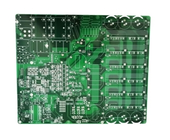
The four layer solar inverter PCB is a printed circuit board designed specifically for solar inverters, mainly used to convert the direct current generated by solar panels into alternating current for household or industrial use. This PCB adopts a four layer design, which can effectively support complex circuit layouts and high-power applications, ensuring the high efficiency and stability of the inverter.
Product Features
1. Four layer design
High density wiring: The four layer structure allows for more complex circuit designs, suitable for high-power and high-frequency applications.
Signal integrity: Through layered design, signal interference is reduced, and the stability and reliability of the circuit are improved.
2. Excellent electrical performance
Efficient Conversion: Optimized circuit design ensures efficient DC to AC conversion, maximizing energy utilization.
Low heat loss: The design considers thermal management, reducing the heat loss of the inverter during operation.
3. High temperature resistance and corrosion resistance
High temperature tolerance: able to withstand the high temperature generated by the inverter during operation, ensuring long-term stable operation.
Anti corrosion materials: using anti-corrosion materials, suitable for various environmental conditions, extending the service life of PCB.
4. Good heat dissipation performance
Heat dissipation design: Reasonable heat dissipation design ensures that the inverter can maintain good operating temperature under high load.
Heat dissipation holes and thermal conductive materials: Adding heat dissipation holes and thermal conductive materials to PCB design further enhances the heat dissipation effect.
Technical Specifications
Number of floors: 4
Board: FR4, SY1000
Plate thickness: 1.6mm
Minimum aperture: 0.50mm
Surface treatment: lead-free tin spraying
Copper thickness: High voltage DC power supply system, inner and outer copper thickness of 2oz,
Copper hole thickness: 25um
Application field
Solar inverters: used for various types of solar inverters, including photovoltaic power generation systems and off grid systems.
Power Conversion: Suitable for the power conversion needs of households, businesses, and industries.
Energy storage system: combined with energy storage equipment to achieve efficient energy management.
production process
1. Design: Use professional software for circuit design and layout to ensure the efficiency and reliability of the circuit.
2. Plate making: Produce a photolithography plate based on the design documents and perform preliminary PCB processing.
3. Etching: Remove excess copper layers to form circuit patterns.
4. Drilling: Drill holes according to design requirements to connect circuits between different layers.
5. Surface treatment: Perform anti oxidation treatment to improve welding performance.
6. Testing: Conduct electrical testing to ensure product quality and performance.
summary
The four layer solar inverter PCB is an indispensable component of solar inverters, widely used in various solar power generation systems due to its excellent electrical performance and high-density design. Whether it's power conversion or energy management, the four layer solar inverter PCB can meet the needs of modern solar energy applications, ensuring users have an efficient energy utilization experience.
Do You have office in shanghai or shenzhen that i can visit?
Answer: We are in Shenzhen.
Will you will attend the fair to show your products?
Answer:; We're planning on it
How long it takes you to provide the designing options for us?
Answer: 3 days
The most common issue is welding, manifested as uneven or virtual welding of the solder joints.
Answer:; It is necessary to strictly control the welding temperature and time, and use high-quality solder
5. Electromagnetic interference problem
Answer: It can be solved by arranging components reasonably and adding shielding layers,
6. There is also a heat dissipation issue
Answer: Generally, it can be improved by installing heat sinks or using high thermal conductivity materials.


