loading


| Availability: | |
|---|---|
| Quantity: | |
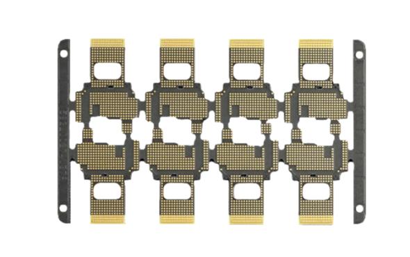
6-layer gold-plated PCB is a high-performance printed circuit board widely used in complex electronic devices such as computers, communication equipment, medical instruments, etc. It is composed of six layers of conductive and insulating materials, and uses immersion gold (ENIG) surface treatment technology to provide excellent electrical performance and welding reliability.
Product Features
1. Multi layer design
High density wiring: The 6-layer design allows for more complex circuit layouts, suitable for high-density and miniaturized electronic products.
Signal integrity: A multi-layer structure helps reduce signal interference and improve signal integrity.
2. Gold immersion surface treatment
Excellent weldability: Immersion gold treatment provides excellent weldability, ensuring the reliability of solder joints.
Oxidation resistance: The gold layer can effectively prevent oxidation and extend the service life of the PCB.
3. Excellent electrical performance
Low signal loss: Good conductivity ensures the stability of signal transmission.
High frequency applications: Suitable for high-frequency circuits to meet the needs of modern electronic products.
4. Heat resistance and corrosion resistance
High temperature tolerance: able to withstand high temperature welding and working environments, suitable for industrial and high-performance applications.
Corrosion resistance: Surface treatment can prevent oxidation and corrosion, extending the service life.
Technical Specifications
Number of layers: 6
Board: FR-4 SY1000
Plate thickness: 1.6+/-0.16mm
Minimum aperture: 0.25mm
Minimum pore copper: 20um
Copper thickness: 1OZ
Minimum line width: 0.15mm
Minimum line spacing: 0.18mm
Surface treatment: Sinking gold+gold fingers
Application field
Computers: motherboards, graphics cards, storage devices, etc.
Communication equipment: routers, switches, base stations, etc.
Medical equipment: monitoring instruments, diagnostic equipment, etc.
Industrial control: automation equipment, control systems, etc.
production process
1. Design: Use professional software for circuit design and layout.
2. Plate making: Produce a photolithography plate according to the design documents.
3. Etching: Remove excess copper layers to form circuit patterns.
4. Drilling: Drill holes according to design requirements to connect circuits between different layers.
5. Surface treatment: Perform immersion gold treatment to improve welding performance and corrosion resistance.
6. Testing: Conduct electrical testing to ensure product quality.
summary
6-layer gold-plated PCB is an indispensable component of modern electronic products, widely used in various high-tech fields due to its excellent electrical performance and reliable solderability. Whether it's computers, communication equipment, or medical instruments, 6-layer gold-plated PCBs can meet the requirements of high performance and high reliability.
common problem:
Do You have office in shanghai or shenzhen that i can visit?
Answer: We are in Shenzhen.
Will you will attend the fair to show your products?
Answer:; We're planning on it
How long it takes you to provide the designing options for us?
Answer: 3 days
Question 4: Can you make 30 wheat thick gold fingers? Answer: It's possible
Question 5: Can you make long and short gold fingers? Answer: Sure.
Question 6: Can you remove residual leads with your golden fingers? Answer: It's possible.


