loading
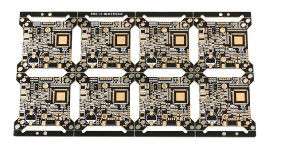
Rigid PCB is a type of printed circuit board widely used in electronic products, with a fixed shape and structure, typically composed of multiple layers of insulating and conductive materials. Rigid PCBs are widely used in various electronic devices, such as mobile phones, computers, household appliances, and industrial equipment, due to their excellent electrical performance, mechanical strength, and durability.
Product Features
1. High strength and stability
Mechanical strength: Rigid PCBs have high resistance to bending and impact, making them suitable for use in harsh environments.
Fixed shape: not easily deformed, suitable for applications that require precise positioning and connection.
2. Excellent electrical performance
Low signal loss: Good conductivity ensures the stability and reliability of signal transmission.
High frequency performance: suitable for high-frequency circuit design, meeting the needs of modern electronic products.
3. Multi layer design
Complex circuits: Supports multi-layer design, enabling more complex circuit layouts and saving space.
Higher connection density: suitable for miniaturization and high-density electronic product design.
4. Heat resistance and corrosion resistance
High temperature tolerance: able to withstand high temperature welding and working environments, suitable for industrial applications.
Corrosion resistance: Surface treatment can prevent oxidation and corrosion, extending the service life.
Technical Specifications
Number of layers: 6
Board: FR-4 SY1000
Plate thickness: 1.6+/-0.16mm
Size: 152mm * 84mm
Minimum aperture: 0.25mm
Minimum pore copper: 20um
Copper thickness: 1OZ
Minimum line width: 0.15mm
Minimum line spacing: 0.18mm
Surface treatment: immersion gold
Application field
Consumer electronics: mobile phones, tablets, televisions, etc.
Computer: motherboard, graphics card, hard drive, etc.
Industrial equipment: automation equipment, instruments, control systems, etc.
Automotive electronics: in car navigation, entertainment systems, sensors, etc.
production process
1. Design: Use professional software for circuit design and layout.
2. Plate making: Produce a photolithography plate according to the design documents.
3. Etching: Remove excess copper layers to form circuit patterns.
4. Drilling: Drill holes according to design requirements to connect circuits between different layers.
5. Surface treatment: Perform necessary surface treatment to improve welding performance and corrosion resistance.
6. Testing: Conduct electrical testing to ensure product quality.
summary
Rigid PCB is an indispensable component of modern electronic products, widely used in various fields due to its excellent mechanical and electrical performance. Whether it is consumer electronics, industrial equipment, or automotive electronics, rigid PCBs can meet the requirements of high performance and high reliability.
1.Do You have office in shanghai or shenzhen that i can visit?
Answer: We are in Shenzhen.
2.Will you will attend the fair to show your products?
Answer:; We're planning on it
3.How long it takes you to provide the designing options for us?
Answer: 3 days
4. Security monitoring PCB signal interference
Answer: Due to improper wiring, poor grounding design, or excessive power noise. The solutions include optimizing wiring, allocating ground and power lines reasonably, and using shielding layers or filters to reduce noise interference.
Insufficient thermal design of layer 5.6 PCB:
Answer: A 6-layer PCB circuit board generates a large amount of heat during operation. If the thermal design is insufficient, it may cause the circuit board to overheat, affecting the normal operation of the circuit. The solution includes adding heat sinks or fins, optimizing the heat dissipation path, and arranging the heat dissipation components reasonably
6. Poor impedance matching of security monitoring PCB
Answer: It causes reflection and loss during signal transmission, affecting circuit performance. The solution includes using impedance calculation tools for impedance matching design, selecting materials and thicknesses reasonably, and optimizing wiring


