loading
Product Overview
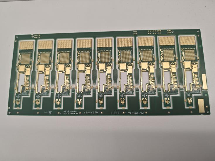
The 8-layer HDI 800G optical communication module dedicated PCB is a high-performance printed circuit board designed specifically for high-speed optical communication signal transmission. It adopts an advanced 8-layer HDI structure design, combined with high-performance Pana M6 substrate and 2u gold deposition surface treatment process, ensuring excellent electrical performance and reliability. This product has high-density wiring and fine manufacturing processes, which can meet the strict requirements of high precision and high reliability for 800G optical communication modules.
Product Features
High density wiring: With an 8-layer structural design, it achieves smaller line widths and spacing (0.075mm/0.075mm), improves wiring density, and meets the needs of complex optical communication signal transmission systems.
Excellent electrical performance: 2u immersion gold surface treatment process provides good conductivity and oxidation resistance, ensuring the stability and reliability of signal transmission.
High reliability: Pana M6 substrate, Tg185, It has excellent mechanical strength and heat resistance, and can work stably for a long time in high temperature environments.
Exquisite solder mask process: The green solder mask and white silkscreen layer not only looks beautiful, but also effectively protects the PCB surface, preventing short circuits and corrosion.
High precision aperture: The minimum aperture is 0.2mm, ensuring precise installation and good electrical connection of the optical communication module.
Technical specifications and parameters
number of layers | 8 |
raw materials | Pana M6,Tg185 |
thickness | 1.0mm |
copper thickness | 1OZ |
color | Green solder mask and white silkscreen |
Minimum line width/line spacing | 0.075mm/0.075mm |
Is there a solder mask present | yes |
Surface treatment method | 2u gold deposit |
Minimum aperture | 0.2mm |
Application field
800G optical communication module: suitable for signal transmission and processing of 800G optical communication modules, providing high-speed data transmission and processing capabilities.
Data Center: Optical communication equipment used in data centers, supporting high-speed data transmission and processing.
Communication base station: Optical communication equipment suitable for communication base stations to ensure stable signal transmission.
High performance computing: an optical communication module used for high-performance computing devices to improve the communication efficiency and reliability of the equipment.
Special production process
1. HDI technology: Interconnection between different copper layers inside is achieved through micro blind hole/buried blind hole technology, improving wiring density and space utilization.
2. Gold deposition process: By electrochemical deposition, a uniform layer of gold is formed on the surface of the PCB, providing excellent conductivity and oxidation resistance.
3. High precision drilling technology: ensuring an accuracy of a minimum aperture of 0.2mm, meeting the precise installation and good electrical connection requirements of optical communication modules.
4. Fine solder mask process: High quality green solder mask and white silkscreen are used to ensure the beauty and functionality of the solder mask layer.
5. Strict quality control: From raw material procurement to production process, strictly control product quality to ensure product reliability and stability.
Product Summary
The 8-layer HDI 800G optical communication module dedicated PCB is an ideal choice for 800G optical communication modules due to its high-density wiring, excellent electrical performance, high reliability, and fine craftsmanship. It can not only meet the strict requirements of high precision and high reliability for 800G optical communication modules, but also work stably for a long time in high temperature environments, providing a solid foundation for the performance improvement and reliability guarantee of optical communication equipment.


