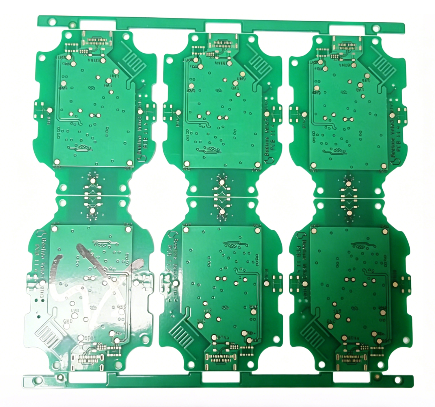
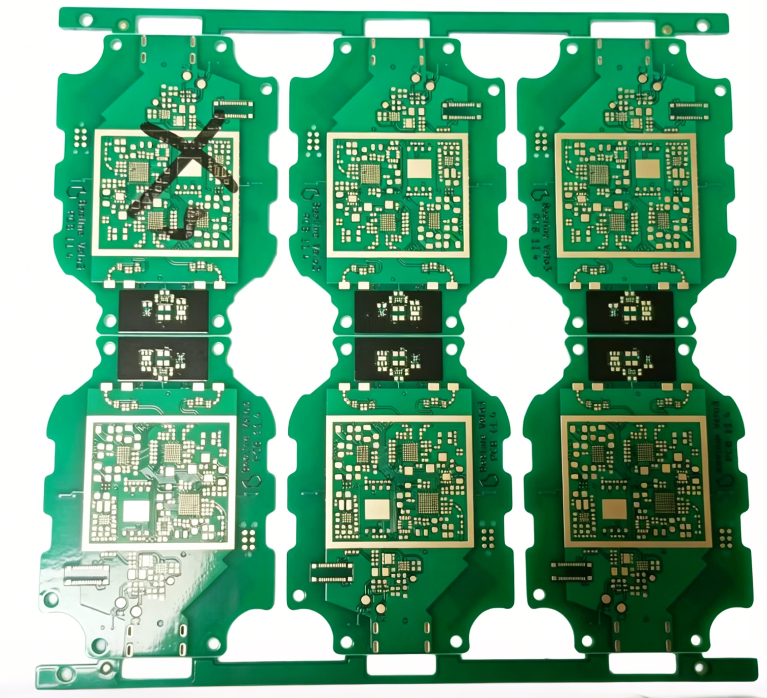
loading
The 6-layer 2nd-order HDI PCB is specially designed for high-density, high-speed signal and miniaturized electronic devices. It adopts high-performance FR-4 TG170 substrate with an ultra-thin board thickness of 0.8mm, balancing structural strength and lightweight requirements. Equipped with green solder mask with white legend and ENIG surface finishing, it greatly enhances oxidation resistance, soldering reliability and signal transmission stability, perfectly meeting high-demand scenarios such as precision main control, communication transmission and embedded systems.
Advanced HDI High-density Wiring: Adopting 6-layer 2nd-order HDI technology, supporting ultra-fine circuits and laser blind & buried vias to accommodate BGA and highly integrated chip layout.
Excellent High-speed Signal Integrity: Low-loss substrate combined with ENIG finishing effectively reduces signal attenuation and crosstalk, ensuring high-speed transmission performance.
Stable Electrical and Mechanical Performance: Reasonable copper thickness configuration with precise impedance control, featuring high temperature resistance and vibration resistance for harsh operating environments.
Miniaturized & Ultra-thin Design: 0.8mm board thickness saves internal device space, ideal for portable and compact products.
High-reliability Eco-friendly Process: RoHS compliant. ENIG plus green solder mask with white legend delivers outstanding oxidation and corrosion resistance for long-term stable operation.
Layers: 6 Layers
Process: 6-layer 2nd-order HDI (Blind & Buried Vias + Laser Drilling)
Substrate: FR-4 TG170
Board Thickness: 0.8mm
Solder Mask: Green Solder Mask with White Legend
Surface Finishing: ENIG (Electroless Nickel Immersion Gold)
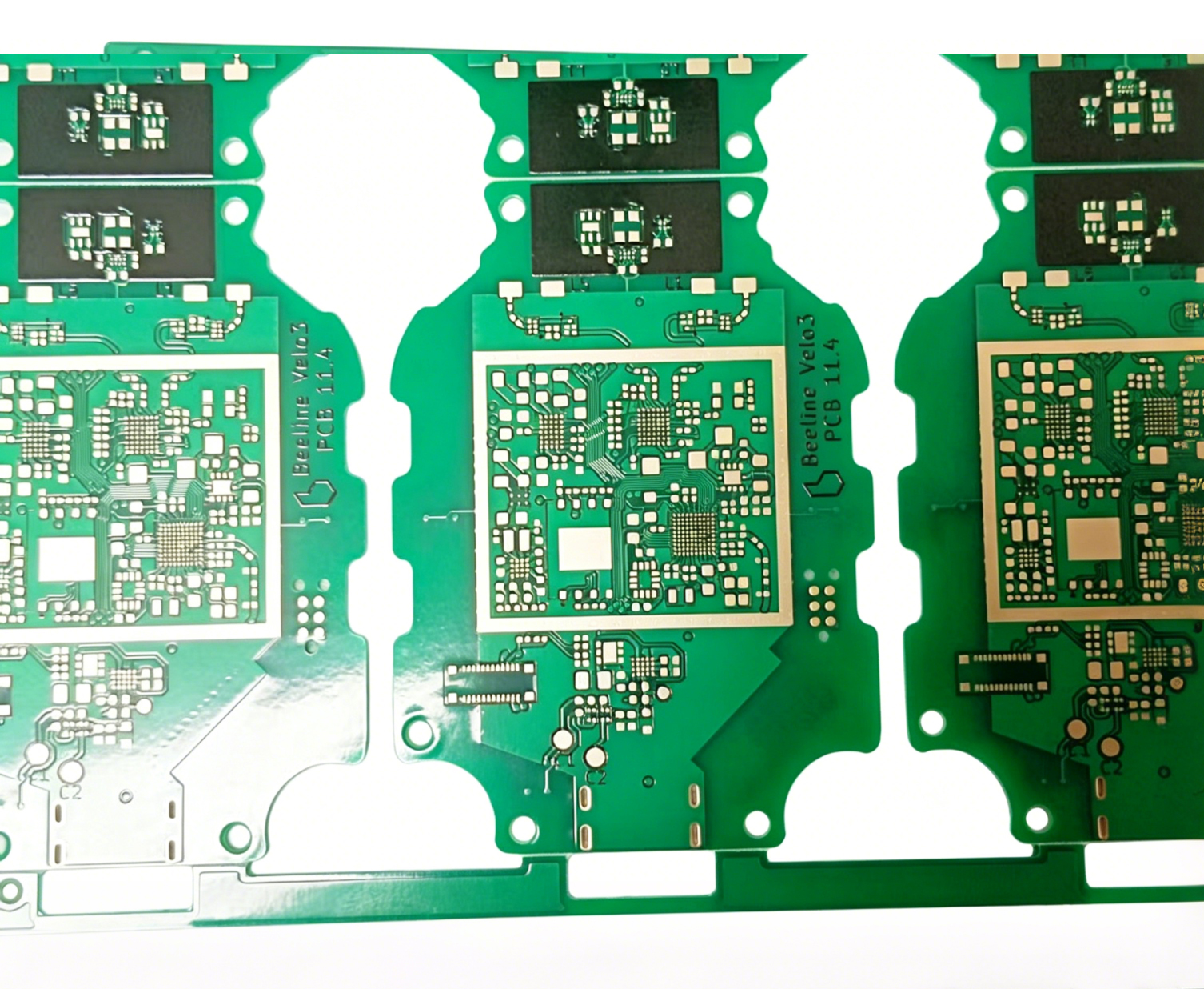
Minimum Line Width / Line Spacing: 0.07mm / 0.075mm
Minimum Aperture: 0.1mm
Minimum BGA Pad: 0.2mm
Copper Thickness: 1oz
Wearable Electronics & TWS: Main control boards for smart watches and earbuds, adapting to ultra-thin space and high-density layout.
Automotive Electronics: Vehicle central control, T-BOX and ADAS small modules, meeting automotive-grade stability standards.
Industrial IoT & Embedded Systems: Industrial gateways, edge computing and sensor main controls, with anti-interference and high temperature resistance.
Consumer Electronics: Mobile modules, portable devices and camera modules with high integration and high-speed signal transmission.
Medical & Security: Compact medical equipment and monitoring modules for high reliability and long service life.
2nd-order HDI Blind & Buried Via Process: Enables multi-layer interconnection to improve wiring density and signal quality.
Laser Drilling Technology: Minimum aperture up to 0.1mm, supporting ultra-fine holes and high-density design.
ENIG Surface Finishing: Low contact resistance, excellent solderability, oxidation and corrosion resistance.
High-precision Etching: Ultra-fine line width and spacing processing to ensure circuit accuracy and impedance consistency.
Green Solder Mask with White Legend: Provides insulation protection and clear marking with elegant appearance and durability.
The 6-layer 2nd-order HDI PCB serves as a core carrier for highly integrated, high-speed and miniaturized devices. Featuring high-density wiring, superior signal integrity, stable electrical performance and ultra-thin reliable design, it is widely applied in smart wearables, automotive electronics, industrial IoT, consumer electronics, medical and security industries. With advanced HDI technology and mature surface treatment, it stands as the preferred solution for high-end precision electronic products.


