loading
The 12 layer communication module PCB circuit board is a high-density, multi-level printed circuit board designed specifically for modern communication equipment. It can support complex circuit layouts and high-frequency signal transmission, and is widely used in fields such as 5G base stations, routers, switches, and IoT devices.
Product Features
1. High level design
2. Adopting a 12 layer structure, providing greater wiring space, supporting complex circuit design and multi signal transmission.
3. Excellent electrical performance
4. The design has optimized signal integrity, reduced signal attenuation and crosstalk, and is suitable for high-frequency applications.
5. Low loss materials
6. Use low dielectric constant and low loss substrates (such as FR-4, PTFE, etc.) to ensure efficient signal transmission.
7. Good thermal management
8. The design takes into account thermal distribution, using heat dissipation holes and thermal conductive materials to ensure stability during high-power operation.
9. High precision manufacturing
10. Adopting advanced manufacturing processes to ensure high circuit accuracy and meet the requirements of complex circuits.
Application Fields
5G communication equipment
Used for 5G base stations, antenna systems, and other communication modules, supporting high-speed data transmission.
network equipment
Applied to network devices such as routers and switches, providing stable network connections.
IoT devices
Suitable for various IoT sensors and controllers, enhancing the communication capabilities of devices.
Industrial Automation
Used for industrial control systems and automation equipment, supporting real-time data transmission and processing.
Technical Specifications
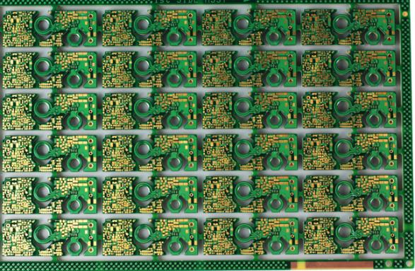
Number of layers: 12
Thickness: 2.0mm
Board used: FR4 SY1000-2M
Solder mask color: green, oil, white letters
Copper thickness: inner 0.5, outer 1OZ
Minimum aperture: 0.4mm
Surface treatment: immersion gold
Application field: Communication
Design and Manufacturing Process
1. Requirement analysis
2. Communicate with customers to understand product requirements and technical specifications, ensuring that the design complies with communication standards.
3. Circuit design
4. Use professional software for circuit design, optimize signal paths, and reduce interference.
5. PCB layout
6. Conduct a 12 layer layout, arrange the position of circuit components reasonably, and ensure signal integrity and power distribution.
7. Production and manufacturing
8. Use high-precision equipment for PCB production to ensure product quality and performance.
9. Testing and Verification
10. Conduct strict electrical performance testing and environmental adaptability testing on finished products to ensure compliance with design requirements.
summary
The 12 layer communication module PCB circuit board is the core component of modern communication equipment, and with its superior performance and wide application prospects, it has become an ideal choice for high-frequency and high-speed communication. We are committed to providing customers with high-quality products and professional technical support to meet the constantly evolving demands of the communication market.
Frequently Asked Questions
1.How far is your factory from the airport?
Answer: 30 kilometers.
2.What is your MOQ?
Answer: 1PCS,
When can I receive a quotation after providing Gerber with the product process requirements?
Answer: PCB quotation within 1 hour.
In the use and maintenance of communication PCB boards, the following problems are often encountered:
Answer: 1 Common open circuit and short circuit problems on circuit boards are usually caused by circuit aging or manufacturing defects, and require careful inspection and professional maintenance to solve;
2. Overheating issues can lead to component burnout or system instability, and introducing heat dissipation design and improving material selection are key factors;
3. Signal interference needs to be reduced by optimizing PCB layout and planning ground wires reasonably.
4. Understanding these issues and their solutions can effectively improve the service life and performance of communication PCB boards.
5. Do you have laser drilling machines,
Answer: Yes, there are.
6. How many layers of HDI circuit boards does your company produce
Answer: We can produce any interconnect PCB circuit board from four layers of first order to higher layers.


