loading
Product Overview
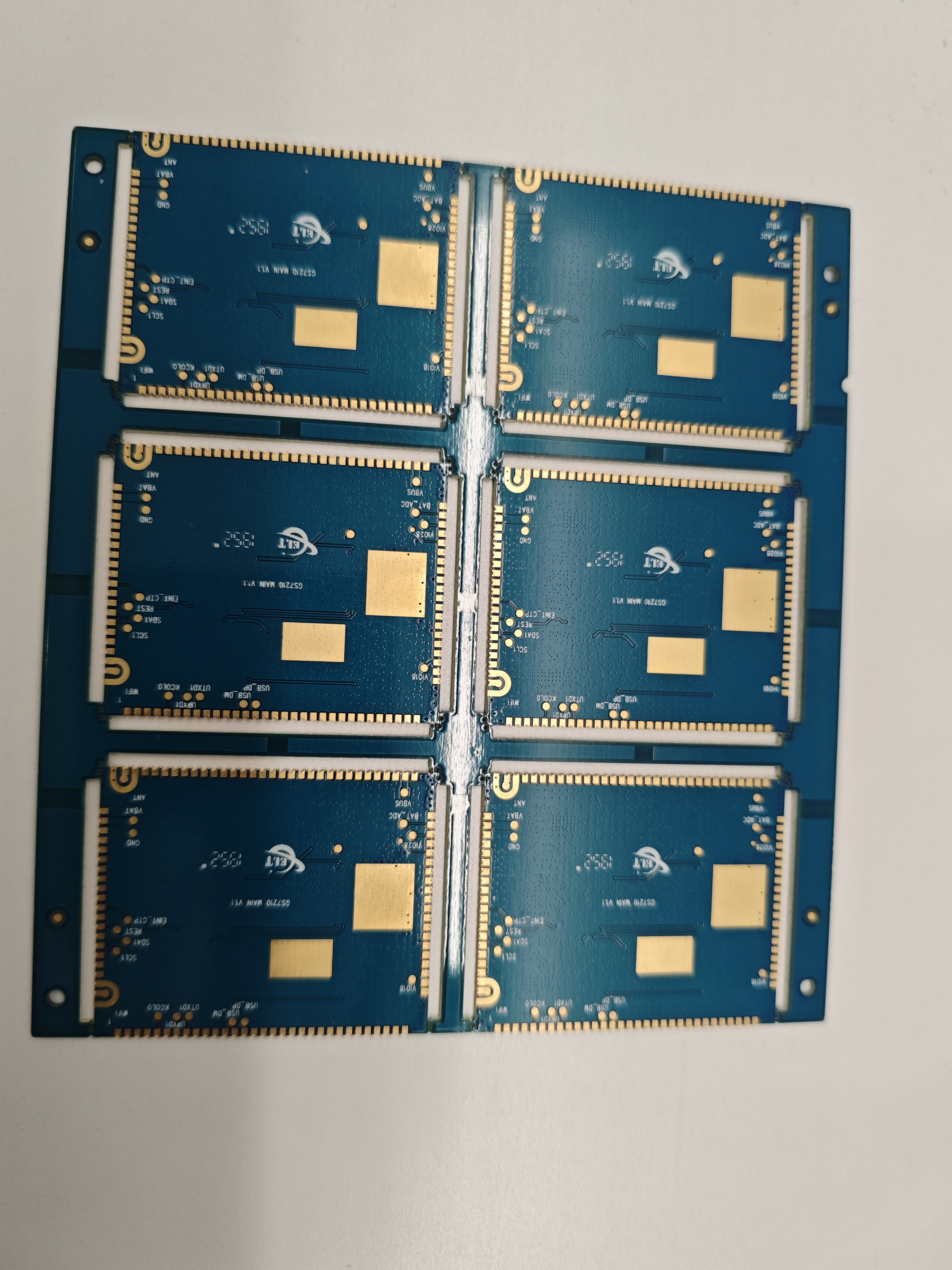
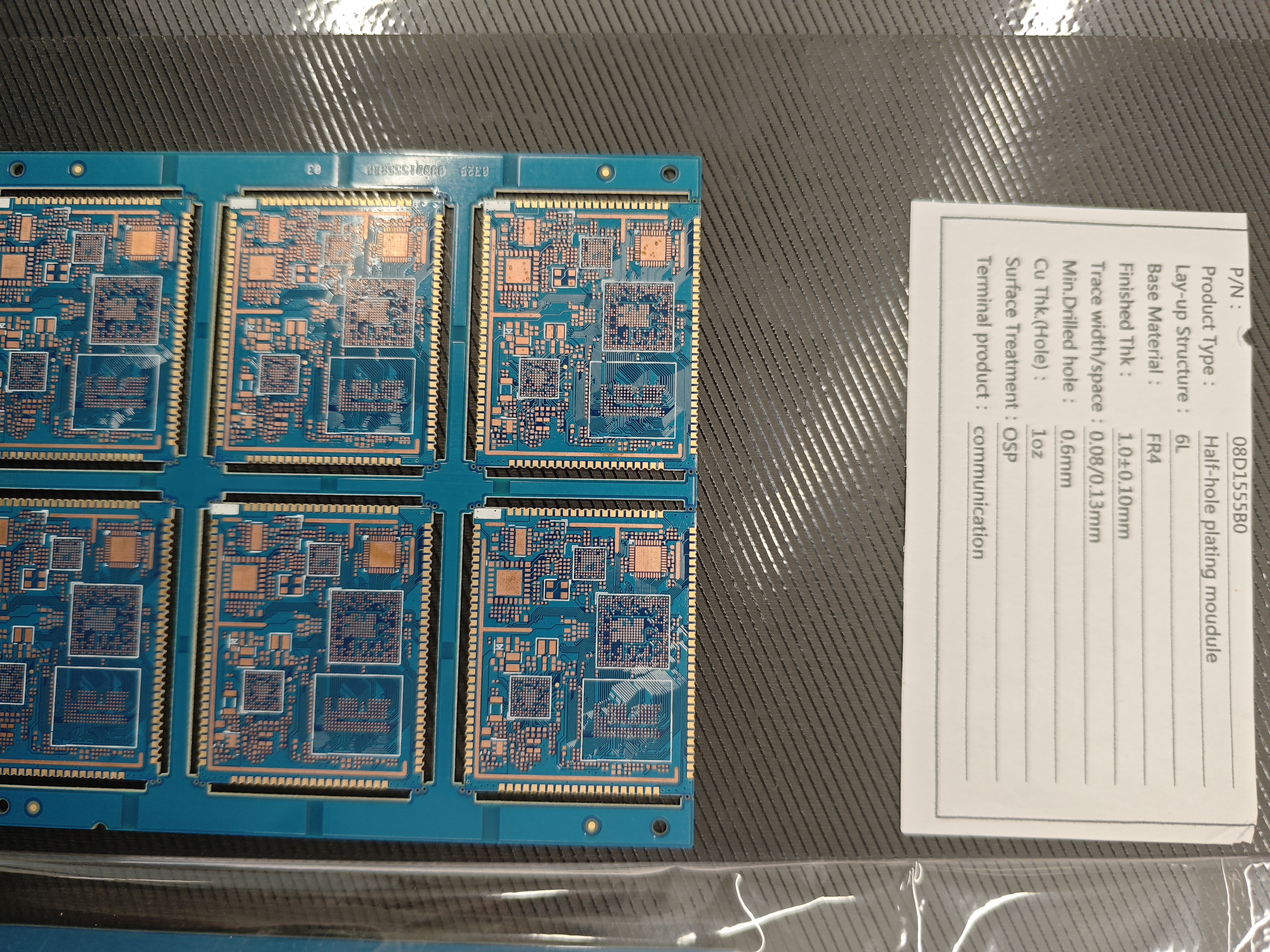
The "6-layer 5G communication system AC PCB" is a high-performance printed circuit board designed specifically for 5G communication systems, which can meet the strict requirements of 5G communication equipment for high-speed signal transmission, high-density wiring, and high reliability. This product adopts advanced manufacturing technology and high-quality materials to ensure low loss and high stability during high-frequency signal transmission, providing solid hardware support for the efficient operation of 5G communication equipment.
Product Features
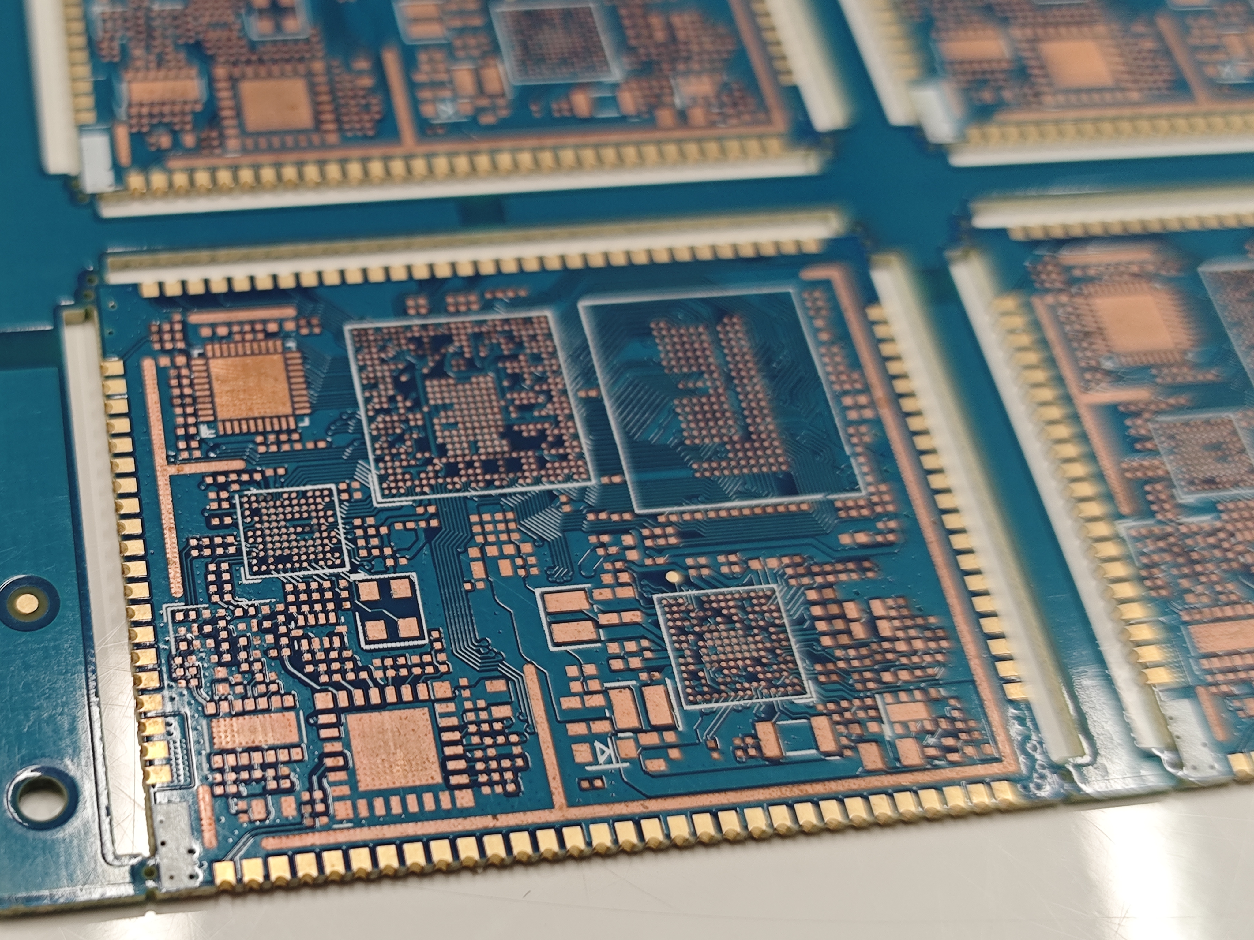
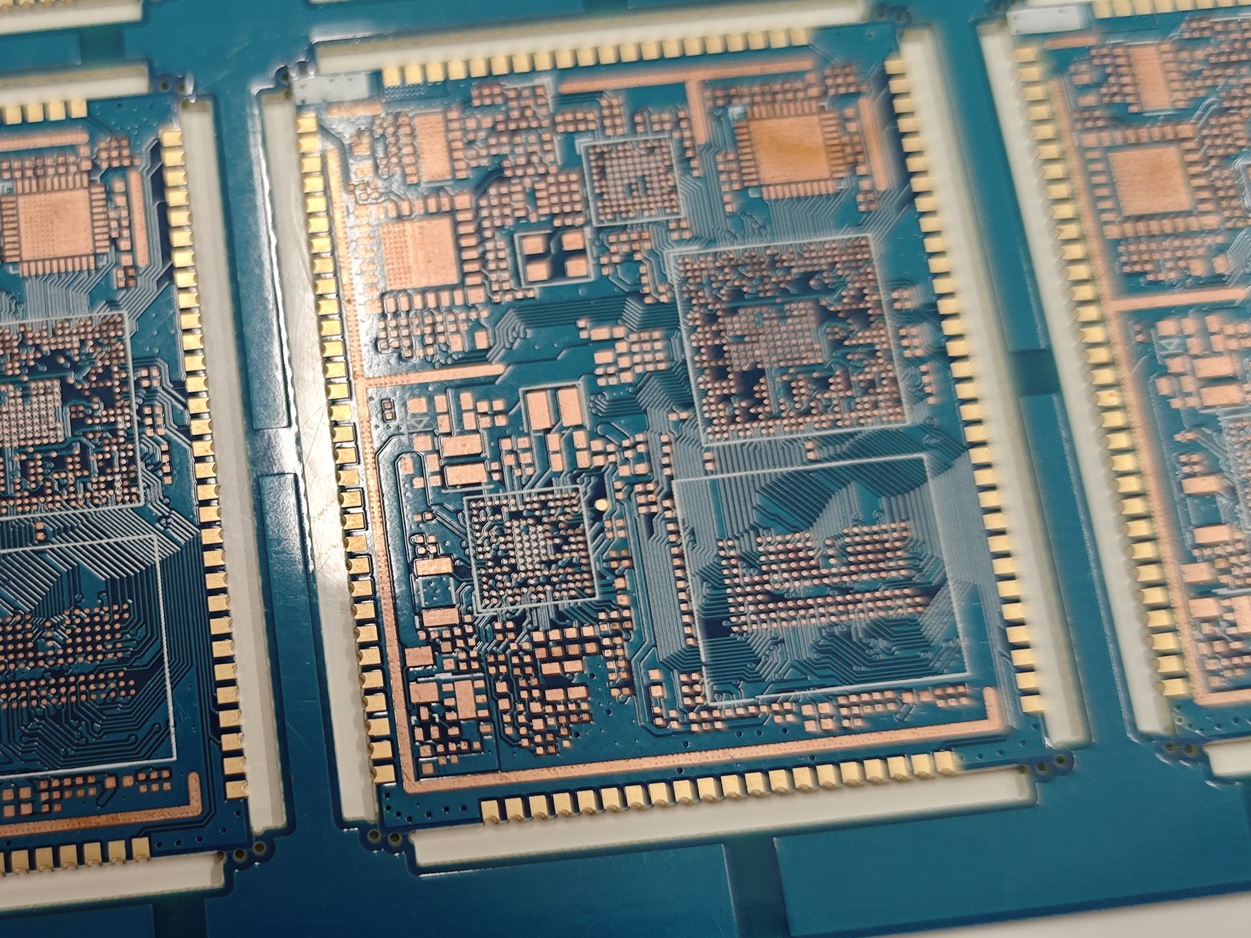
1. Excellent high-frequency signal transmission performance: Using high-quality FR-4 substrate and a 6-layer structural design, it can effectively reduce signal transmission loss and ensure the integrity of high-frequency signals.
2. High density wiring capability: With a fine wiring capability of 0.08mm line width and 0.13mm line spacing, combined with a minimum aperture of 0.6mm, high-density wiring is achieved to meet the needs of complex circuit design.
3. Good heat dissipation performance: The 1.0mm board thickness and 1oz copper thickness design help to dissipate heat quickly and ensure the stability of the equipment during high load operation.
4. High reliability: The blue oil white solder mask process and OSP surface treatment provide good electrical insulation and anti-corrosion performance, extending the service life of the PCB.
5. Strong compatibility: Suitable for various 5G communication devices, it can seamlessly integrate with existing communication systems to achieve efficient data transmission and signal processing.
Technical Specifications
number of layers | 6 |
substrate | FR-4 |
thickness | 1.0mm |
color | Blue solder mask and white silkscreen |
Minimum line width/line spacing | 0.08mm/0.13mm |
Is there a solder mask present | have |
Surface treatment method | Sinking Gold 1U |
copper thickness | 1oz |
Application Areas
5G base station equipment: used for RF modules, baseband processing units, etc. in 5G base stations to achieve high-speed signal reception and transmission.
5G terminal devices: suitable for 5G smartphones, tablets, IoT devices, etc., providing stable signal transmission and data processing capabilities.
Industrial 5G communication: used in industrial automation equipment to achieve high-speed communication and data exchange between devices.
Intelligent transportation system: supports 5G communication modules in vehicle networking applications to achieve real-time data transmission between vehicles and infrastructure.
Medical communication equipment: A 5G communication module used in remote medical devices to ensure fast transmission and high reliability of medical data.
The special production process adopted
1. Fine wiring process: High precision photolithography and etching techniques are used to ensure precise implementation of 0.08mm line width and 0.13mm line spacing, meeting the requirements of high-frequency signal transmission.
2. Multilayer lamination process: Advanced multi-layer lamination technology ensures the interlayer alignment accuracy and electrical performance of the 6-layer board, reducing signal transmission delay.
3. OSP surface treatment process: OSP (organic solder mask) surface treatment is used to provide good oxidation resistance and soldering performance, ensuring the reliability of PCB in long-term use.
4. High precision drilling technology: Ensure precise machining of the minimum aperture of 0.6mm, improve wiring density and overall performance of the circuit board.
5. Blue solder mask and white silkscreen process: this design not only provides good electrical insulation performance, but also effectively prevents solder bridging during the production process, improving production yield.
Product Summary
The "6-layer 5G communication system AC PCB" provides an ideal hardware solution for 5G communication equipment with its excellent high-frequency signal transmission performance, high-density wiring capability, and high reliability. This product adopts advanced manufacturing technology and high-quality materials to ensure low loss and high stability during high-frequency signal transmission. Whether in 5G base stations, 5G terminal equipment, or industrial automation and intelligent transportation systems, this PCB can provide solid guarantees for the efficient operation of equipment, and help promote the widespread application and development of 5G communication technology.


