loading
Product Overview
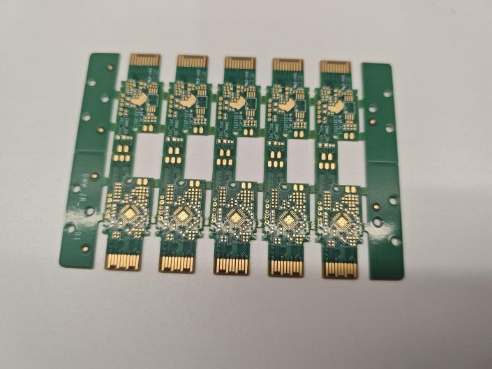
The 4-layer small optical communication instrument dedicated PCB is a high-performance printed circuit board designed specifically for small optical communication signal transmission systems. It adopts an advanced 4-layer structural design, combined with high-performance FR-4 substrate and gold deposition surface treatment process, ensuring excellent electrical performance and reliability. This product has high-density wiring and fine manufacturing processes, which can meet the strict requirements of small optical communication instruments for high precision and high reliability
Product Features
1. High density wiring: 4-layer structural design, achieving smaller line width and spacing (0.08mm/0.28mm), improving wiring density, and meeting the needs of complex optical communication signal transmission systems
2. Excellent electrical performance: The gold-plated surface treatment process provides good conductivity and oxidation resistance, ensuring the stability and reliability of signal transmission
3. High reliability: FR-4 substrate has excellent mechanical strength and heat resistance, and can work stably for a long time in harsh environments
4. Fine solder mask process: The green solder mask and white silkscreen layer not only looks beautiful, but also effectively protects the PCB surface, preventing short circuits and corrosion
5. High precision aperture: The minimum aperture is 0.56mm, ensuring precise installation and good electrical connection of optical communication instruments
Technical specifications and parameters
number of layers | 4 |
raw materials | FR-4 |
thickness | 1.0mm |
copper thickness | 1oz |
color | Green solder mask and white silkscreen |
Minimum line width/line spacing | 0.08mm/0.28mm |
Is there a solder mask present | yes |
Surface treatment method | gold immersion |
| Minimum aperture | 0.56mm |
Application field
Small optical communication signal transmission system: suitable for signal transmission and processing of small optical communication equipment, such as optical modules, optical transceivers, etc
Data Center: Optical communication equipment used in data centers to provide high-speed data transmission and processing capabilities
Communication base station: Optical communication equipment suitable for communication base stations to ensure stable signal transmission
Industrial automation: Optical communication modules used in industrial automation equipment to improve the communication efficiency and reliability of the equipment
Special production process
1. Gold deposition process: By electrochemical deposition, a uniform gold layer is formed on the surface of the PCB, providing excellent conductivity and oxidation resistance
2. High precision drilling technology: ensuring an accuracy of a minimum aperture of 0.56mm, meeting the precise installation and good electrical connection requirements of optical communication instruments
3. Fine solder mask process: High quality green oil and white silkscreen are used to ensure the beauty and functionality of the solder mask layer
4. Strict quality control: From raw material procurement to production process, strictly control product quality to ensure product reliability and stability
Product Summary
The 4-layer small optical communication instrument dedicated PCB has become an ideal choice for small optical communication signal transmission systems due to its high-density wiring, excellent electrical performance, high reliability, and fine craftsmanship. It can not only meet the strict requirements of high-precision and high reliability for small optical communication instruments, but also work stably in various environments for a long time, providing a solid foundation for the performance improvement and reliability guarantee of optical communication equipment.


