loading
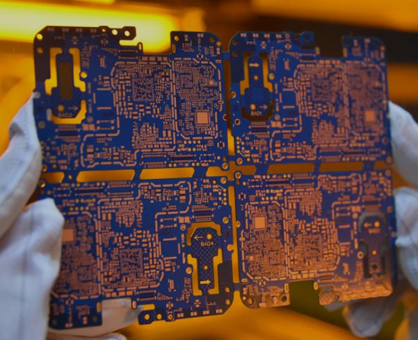
A 6-layer second-order HDI (high-density interconnect) PCB board is a printed circuit board designed specifically for high-end electronic devices such as smartphones. This PCB board adopts advanced manufacturing technology, which can support complex circuit design and high-performance electronic functions, meeting the demands of modern mobile phones for miniaturization, lightweight, and high performance.
Product Features
1. High density interconnection
Multi layer design: The 6-layer structure provides more wiring space, suitable for the design of complex circuits.
Micro hole technology: using micro hole technology (such as blind holes and buried holes), effectively improving wiring density and reducing PCB area.
2. Superior electrical performance
Low resistance and low inductance: Optimized circuit design and material selection ensure efficient and stable signal transmission.
High frequency performance: suitable for high-frequency signal transmission, meeting the needs of modern communication and data processing.
3. Lightweight design
Miniaturization: HDI technology enables PCB boards to be thinner and lighter, suitable for the design requirements of modern mobile phones.
Space saving: High density layout reduces the footprint of PCB and leaves more space for other components.
4. Good heat dissipation performance
Heat dissipation design: Reasonable heat dissipation design ensures that the PCB can maintain good working temperature under high load.
Thermal conductive material: Using thermal conductive materials to enhance heat dissipation and extend product life.
Technical Specifications
Layer 6
Product Structure 1+4+1
Plate thickness 0.8 ± 0.8mm
Material EM-285
Line width/line spacing 0.06/0.063mm
Minimum laser drilling aperture 0.1mm
Surface treatment: nickel gold deposition
Application field
Smartphones: Widely used as motherboards and accessory circuit boards for various types of smartphones.
Tablet computer: High performance circuit design suitable for tablet computers.
Wearable devices: There are also applications in smartwatches and other wearable devices.
production process
1. Design: Use professional PCB design software for circuit design to ensure efficient and reliable circuits.
2. Plate making: Produce a photolithography plate based on the design documents and perform preliminary PCB processing.
3. Etching: Remove excess copper layers to form circuit patterns.
4. Drilling: Drill holes according to design requirements to connect circuits between different layers.
5. Surface treatment: Perform anti oxidation treatment to improve welding performance.
6. Testing: Conduct electrical testing to ensure product quality and performance.
summary
The 6-layer second-order HDI PCB board is an indispensable key component in modern mobile phones, widely used in smartphones and other high-end electronic devices due to its high-density design and superior electrical performance. It not only meets the needs of miniaturization and lightweighting, but also ensures efficient signal transmission and good heat dissipation performance, which is an important foundation for achieving high-performance electronic products.
Frequently Asked Questions
1. Is the mobile phone PCB design unreasonable?
Answer: If the circuit design lacks a reasonable layout, it may lead to signal interference and unstable transmission, thereby affecting the performance of the entire mobile phone. Therefore, in the design phase, we need to fully consider the rationality of the position and routing of each component.
2. Is the selection of sheet metal qualified?
Answer: The substrate and soldering materials of PCB are crucial for the reliability of the circuit. Using inferior materials not only affects their lifespan, but may also cause malfunctions in high temperature or high humidity environments.
3. Can lax process control also lead to many problems?
Answer: During the production process, factors such as uneven coating thickness and inaccurate milling may have a negative impact on the performance of PCBs. Therefore, strict control of production processes is the key to ensuring quality.
4. The testing process cannot be ignored, as many issues are often exposed during testing?
Answer: Through a comprehensive testing process, we can promptly identify and correct issues to ensure the product's qualification rate.
5: How far is your factory from the airport?
Answer: 30 kilometers.
6.What is your MOQ?
Answer: 1PC
When can I receive a quotation after providing Gerber with the product process requirements?
Answer: PCB quotation within 1 hour.


