loading
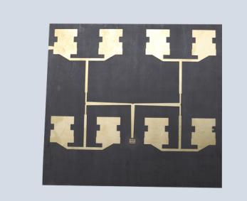
One The double-sided 5G antenna PCB circuit board is a high-performance printed circuit board designed specifically for 5G communication technology, with the characteristics of double-sided wiring, which can meet the needs of 5G networks for high-frequency and high-speed signal transmission. This product is widely used in 5G base stations, smartphones, IoT devices, and other wireless communication devices.
Product Features
1. High frequency performance
2. The design supports a frequency range of up to 30GHz, ensuring stable signal transmission within the 5G frequency band.
3. Double sided wiring design
4. Circuit wiring can be carried out on both sides, providing greater design flexibility and higher circuit density.
5. High quality materials
6. Using low dielectric constant and low loss substrates (such as PTFE, FR-4, etc.) effectively reduces signal attenuation and reflection.
7. High heat dissipation performance
8. Design a reasonable heat dissipation structure to ensure stability during high-power operation and extend the service life of the equipment.
9. Precision manufacturing process
10. Adopting advanced manufacturing technology to ensure high circuit accuracy and suitability for complex circuit design.
Application field
5G base station: an antenna system used for 5G base stations, supporting high-speed data transmission and wide coverage.
Smartphone: Integrated into 5G smartphones, providing stable network connectivity.
IoT devices: Various 5G IoT sensors and controllers to enhance the communication capabilities of devices.
Automotive Electronics: In car 5G communication module, supporting autonomous driving and vehicle networking applications.
Technical Specifications
Number of layers: 2
Plate thickness: 0.6mm
Materal: Teflon
Minimum aperture: 0.8mm
Minimum line width/spacing: 0.12mm
Outer copper thickness: 1OZ
Surface treatment: immersion gold
Design and Manufacturing Process
1. Requirement analysis
2. Communicate with customers to understand product requirements and technical specifications, ensuring that the design complies with 5G standards.
3. Circuit design
4. Use professional software for circuit design, optimize signal paths, and reduce interference.
5. PCB layout
6. Conduct double-sided layout and arrange the positions of antennas and other circuit components reasonably.
7. Production and manufacturing
8. Use high-precision equipment for PCB production to ensure product quality and performance.
9. Testing and Verification
10. Conduct strict electrical performance testing and environmental adaptability testing on finished products to ensure compliance with design requirements.
summary
The double-sided 5G antenna PCB circuit board is a key component for implementing 5G communication technology. With its superior performance and wide application prospects, it has become an indispensable part of modern wireless communication devices. We are committed to providing customers with high-quality products and professional technical support to meet the constantly evolving demands of the 5G market.
common problem:
1, How far is your factory from the airport?
Answer: 30 kilometers.
2.What is your MOQ?
Answer:; 1PCS,
3. Question: After providing Gerber with the product process requirements, when can I receive a quotation?
Answer: PCB quotation within 1 hour.
4. Signal integrity issues
Answer: With the increasing complexity of design, 5G devices may use high-density interconnect (HDI) PCBs with thinner wiring and higher connection pad density. These finer traces may cause signal integrity issues when transmitting high-speed signals.
5. Irregular impedance phenomenon
Answer: Due to various factors such as wire size, width, and cross-section, impedance abnormalities may occur on HDI PCBs, leading to signal loss.
6. Electromagnetic interference and crosstalk
Answer: In order to integrate multiple antenna array units (AAUs), more complex technologies such as multiple input multiple output (MIMO) must be handled. In addition, 5G design will require more base stations and antenna arrays, making electromagnetic interference, crosstalk, and parasitic capacitance key issues.
7. Circuit reliability issues
Answer: Poor process control is not only a problem for technical personnel, but also a problem in the process of building the value chain. The control content of design engineers, procurement engineers, and inspection processes should be designed based on the key indicators of the device to ensure manufacturing reliability.


